Anodic Bonding
Wafer Bonding
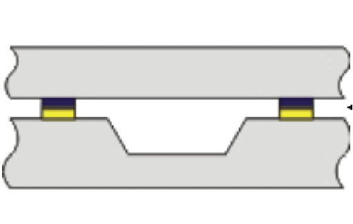
MEMS uses Wafer Bonding technology to assemble the fabricated wafers with different mechanical structures in batches, so as to realize more complex 3D structures. The traditional machining method is to product the mechanical parts by turning, grinding, throwing and other processes, and then realize more complex mechanical structures or systems through assembly. The assembly method of MEMS fabrication is completely different. Common MEMS methods include anodic, direct, metal, reactive and polymer bonding.
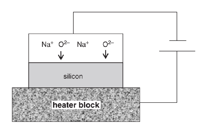
Anodic Bondingis used to bond glass with metal or semiconductor. The negative space charge of the glass and the induced positive charge of the metal or semiconductor attract each other due to static electricity. Direct Bonding, directly bonds two or more clean wafers together under high temperature conditions without intermediate adhesives and electric fields. It is sometimes necessary to combine the processed substrate and the temporary carrier, then to separate them after the thinning process, which need Temporary bonding and debonding technologies. Our Wafer Bonding technology is world-leading.


