Vias
Through substrate vias are interconnection technologies that connects circuits on different surfaces of a wafer, passing vertically through the substrate to conduct electrical signals from one side of the wafer to the other.
Through substrate vias generally consists of a via etched on the substrate, a conductor, and an insulator that separates the conductor from the substrate. According to the different configuration, vias can be divided into different types. Conductor materials can be monocrystal silicon, polycrystalline silicon, as well as Cu, Ti, Au, Al, Ni and other metals. The insulator material can be SiO2, polymer, etc. The resistance of the vias is much smaller than the internal resistance in many MEMS devices, so that the vias can be used to move the lead bonding pad to the CAP. This will help area and reduces parasitic capacitance and other losses (see Figure 1).

图1:使用TXV技术将芯片面积从2×2mm缩小至1×1mm,可大幅增加Die数量
TXVThrough substrate vias are used in Chiplet, CMOS-MEMS 3D and 2.5D integration, and wafer-level packaging. The applied solution has the advantages of high performance, multi-function, low cost, more reliable, small package size, Etc, which deeply promotes the technology progress of MEMS industry.
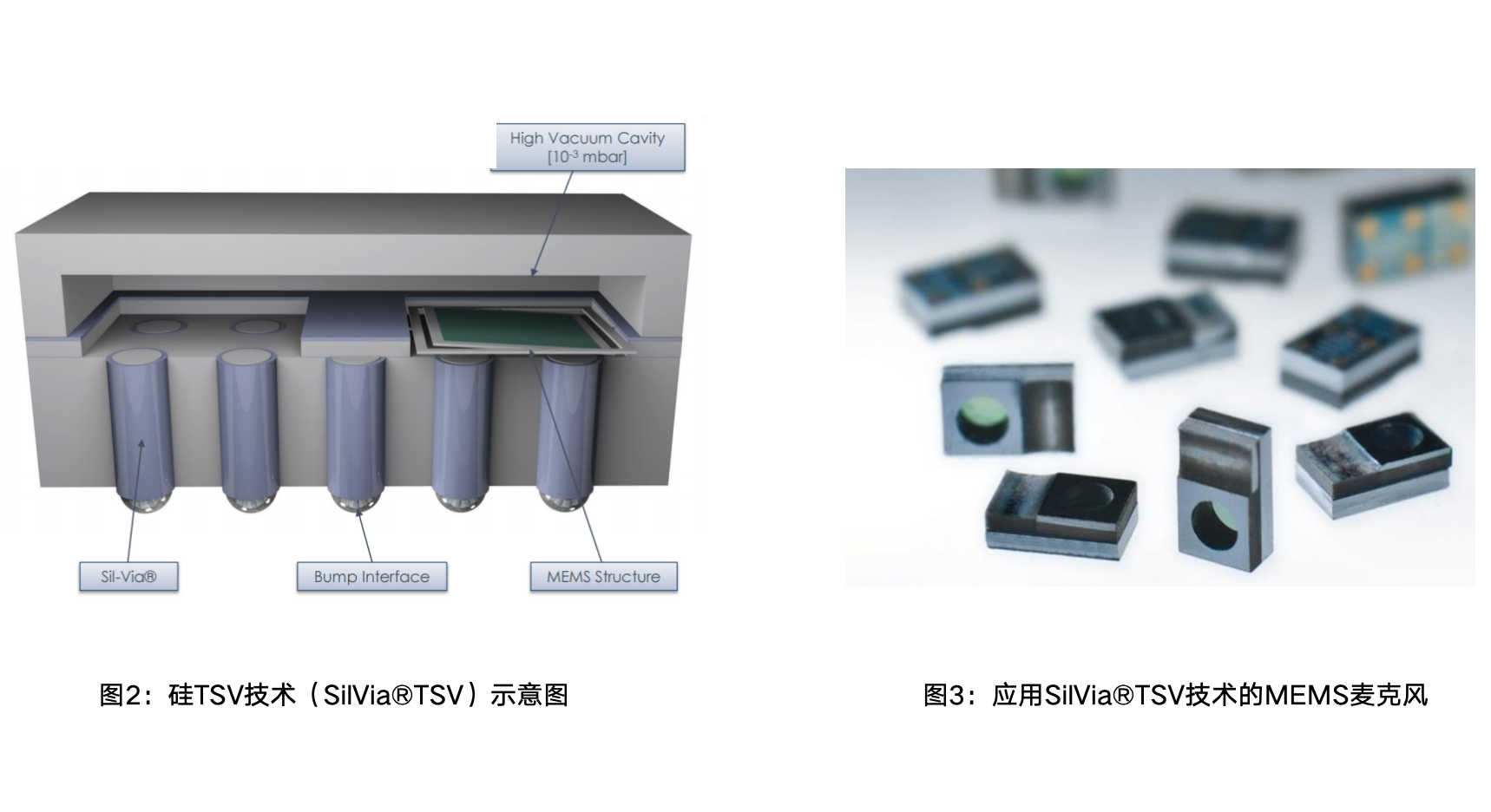
Silex began to develop SilVia®TSV (All-silicon Through Silicon Via) technology in 2003. In 2004, the technology was first applied to the MEMS microphones in mobile phones, resulting in Silex's leading position in the TSV field (see Figure 2 and Figure 3). SilVia®TSV features full-wafer thickness, as well as conductor columns surrounded by insulating material, which facilitates the formation of robust low-resistance interconnect structures and avoids stresses due to mismatches in thermal expansion coefficients between silicon and metal. In 2006, SilVia®TSV, as a process platform, started to be used in the volume production of MEMS devices.

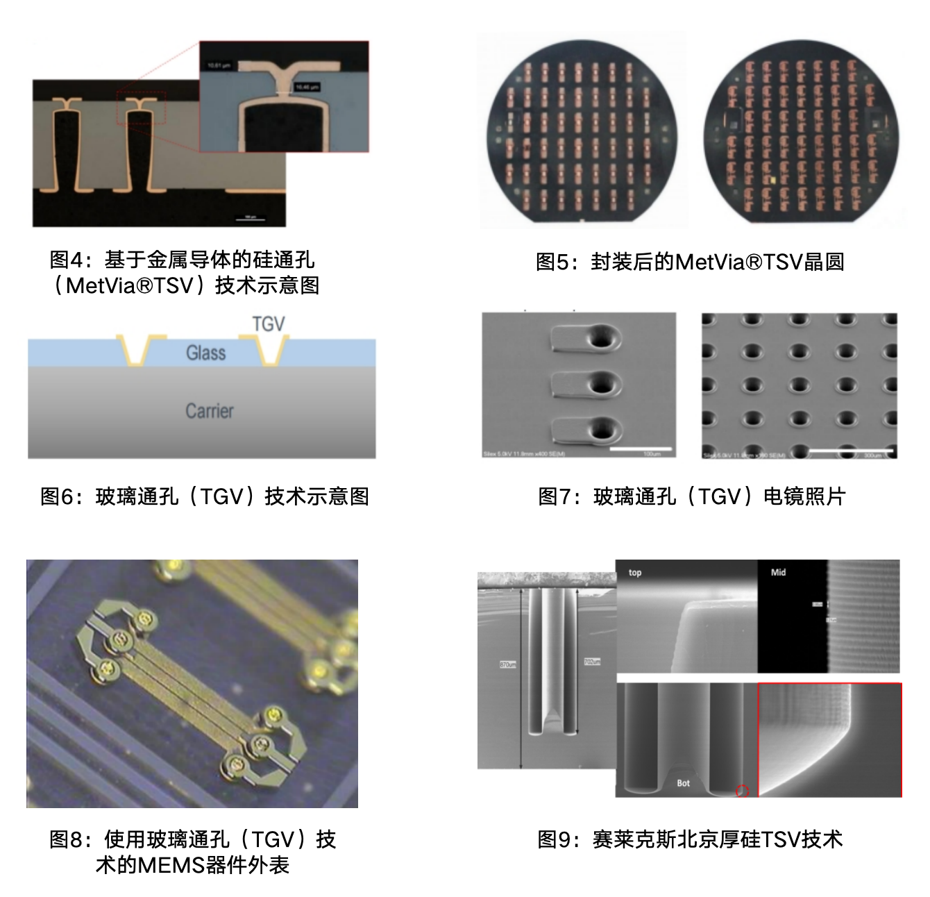
Subsequently, Silex developed MetVia®TSV (Metal Through Silicon Via). The metal conductor structure improved the reliability of vias to produce low-resistance MEMS devices. In 2014, along with the emergence of light and thin devices, Glass materials are used more widely. Silex developed TGV (Through Glass Via), which is used to produce low-resistance devices for high voltage and high frequency applications, so as to make better use of the physical characteristics of glass and reduce the losses of circuits. Silex Beijing has also mastered advanced TSV technology through independent research and development.


